


Intel Panther Lake-H high-res die shot emerges — image show 18A compute tile, Xe3 GPU tile in new X-series processors
Panther Lake's secretes unveiled.
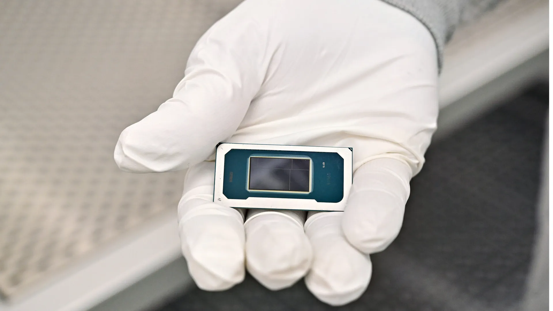
While Intel formally introduced its Core Ultra 300-series processors codenamed Panther Lake-H in January, and even with shipments of several SKUs to partners, it has never revealed its die shots. Fortunately, Kurnal-Insights.com (a website ran by @KurnalSalts) has filled the gap and published annotated die shots of all three tiles that make up Intel's Panther Lake-H processor, including the compute tile made on 18A process technology, the Xe3 graphics tile, and the I/O tile.
Panther Lake-H's compute tile (or system-on-chip tile, as Kurnal calls it) integrates four high-performance Cougar Cove cores with 3 MB L2 cache designed to run at up to 5.1 GHz. In addition, the main compute tile also packs eight space-efficient Darkmont cores running at up to 3.8 GHz and four low-power Darkmont cores operating at up to 3.7 GHz. As far as we can tell, there are no physical differences between Darkmont E-core cluster with 4 MB L2 cache and Darkmont LPE-core cluster with 4 MB L2 cache. Yet, the 18 MB L3 cache split into three slices to serve nearby cores faster is located close to the P-core and E-core clusters, far away from the LPE cluster. NPUs — split into three slices — also have their own 4.5 MB of cache.
Splitting L3 and NPUs into slices enables Intel to disable a defective slice without affecting others in a bid to get a sellable die, albeit offering lower performance.
Intel Panther lake-H DieshotThanks by 万扯淡 Decaphigh pixel Dieshot in my websitehttps://t.co/SOHGS0eViBCPU 14.32x8.04x0.18mmGPU 8.14x6.78x0.2mmIOD 12.44x4.00x0.18mmKurnal will try to change the CPU Die pic.twitter.com/Bmp6Iomlz7March 5, 2026
What is interesting is that the 128-bit DDR5/LPDDR5X-9600 memory controller also has an 8MB memory side cache (MSC), which job is to buffer memory traffic and reduce latency/bandwidth pressure when many cores (or other execution units inside the compute tile, such as NPUs) access RAM simultaneously. Panther Lake is not Intel's first use of a memory-side cache–type structure, though earlier concepts (e.g., CrystalWell L4 cache) were implemented in a considerably different way and their purpose has evolved over time. Therefore, we cannot compare Panther Lake's memory side cache to Apple's system-level cache, which acts like the last level cache for the whole SoC, which is not the case with Intel's MSC.
Another interesting feature of the compute tile are the integrated media and display engines. Such an arrangement enables Intel to attach various GPUs and I/O dies while maintaining key functionality inside the compute tile, which provides the company some additional flexibility with CPU configurations.
In general, the compute tile resembles Intel CPUs released in the recent years, which almost certainly means ring bus interconnect. Yet, the SoC tile also has high-performance interfaces that connect to GPU and I/O die tiles.
As for the GPU tile, it integrates 12 Intel Xe3 clusters and 16MB of L2 cache implemented in eight tiles, which again allows Intel to disable faulty GPU clusters or cache tiles to improve yield of sellable chips.
Get Tom's Hardware's best news and in-depth reviews, straight to your inbox.
The I/O tile is no less interesting than the SoC tile itself as it carries a Thunderbolt 5 controller along with two TB 5.0 PHYs that occupy a significant part of the die. In addition, the IOD carries a Wi-Fi/Bluetooth controller and appropriate physical interfaces, PCIe 5.0 x4 PHY, two PCIe 4.0 x4 PHYs, and USB PHYs. Perhaps, the IOD is the only Panther Lake's tile that can be binned in a bid to get a sellable die with disabled defective parts. If something breaks here, it most likely means that the whole die must be scrapped.

Follow Tom's Hardware on Google News, or add us as a preferred source, to get our latest news, analysis, & reviews in your feeds.

Anton Shilov is a contributing writer at Tom’s Hardware. Over the past couple of decades, he has covered everything from CPUs and GPUs to supercomputers and from modern process technologies and latest fab tools to high-tech industry trends.
-
usertests ReplyAs for the GPU tile, it integrates 12 Intel Xe3 clusters and 16MB of L2 cache implemented in eight tiles
That's huge for the graphics. No wonder it's so fast. -
Notton If I did my math right...Reply
GPU die: 55.19mm²
CPU die: 115.13mm²
I/O die: 49.76mm²
That GPU is quite small for its capabilities.
On the other hand, Strix Halo is 307.58mm² for 40CU GPU + mem controller + I/O, and with 2x 67.02mm² CCDs.
Yes, I'm aware the node size is different.
I find it interesting how AMD and Intel differ in how they break up the tiles. -
TerryLaze Reply
Most people don't use half of the features their system has...Dustyboy1492 said:Lot's of real estate for NPU's that most people don't use.
Also all the things on a CPU are there to make sales happen and if NPUs drive sales then job successfully done. -
Gururu The big question that has vaguely been answered, but hardly definitively, is that being the first 2nm class chip on the market, is it living up to what the technology was expected to provide? I am not even sure what smaller and denser is supposed to offer, can anyone elaborate on whether PTL is meeting those expectations?Reply -
beyondlogic ReplyNotton said:If I did my math right...
GPU die: 55.19mm²
CPU die: 115.13mm²
I/O die: 49.76mm²
That GPU is quite small for its capabilities.
On the other hand, Strix Halo is 307.58mm² for 40CU GPU + mem controller + I/O, and with 2x 67.02mm² CCDs.
Yes, I'm aware the node size is different.
I find it interesting how AMD and Intel differ in how they break up the tiles.
That's good cause that will produce higher yields